Views: 194 Author: Site Editor Publish Time: 2021-06-22 Origin: Site
In the field of optical communication technology, PLC is the abbreviation of Planar Lightwave Circuit. It is a variety of optical waveguide structures prepared based on integrated optical technology. Technically, functional devices that can be realized include directional couplers DC and Y branches Multimode interference coupler MMI, arrayed waveguide grating AWG, optical comb filter ITL, Mach-Zehnder MZ electro-optic modulator, thermo-optic tunable attenuator TO-VOA, thermo-optic switch TO-SW, etc.
In the optical communication industry, PLC devices that are widely used mainly include optical splitters, AWG, MZ electro-optic modulators, TO-VOA, etc. Among them, optical splitters are optical splitters based on Y-branch series and parallel connections, such as a 1 An optical splitter with ×16 ports requires 15 Y splitters. AWG is a 1×N port device, which can separate dozens of input wavelengths to different output ports. MZ modulators based on lithium niobate optical waveguides are currently the most mainstream modulator solution. Silicon optical modulator technology has matured and has become the first choice for high-speed modulators above 50G. TO-VOA based on PLC technology is combined with AWG to form a wavelength division multiplexer/demultiplexer VMUX module with channel equalization function.

There are many kinds of optical communication devices that are widely used based on PLC technology. But in the industry, PLC splitter usually refers to an optical splitter. It is an optical passive device that is most widely used in FTTH networks. After the Internet bubble in 2000, the optical communications industry entered a period of depression. Around 2004, Japan took the lead in investing and constructing FTTH as an infrastructure when the application scenarios had not yet appeared. With China joining after 2008, FTTH construction reached its peak around 2012.
FTTH usually adopts the passive optical network PON, and its core is the PLC optical splitter. It is widely laid in various commercial buildings and residences. In life experience, the closest thing to us is the "cat" tail of the home modem. It is upgraded from the early twisted pair to the current fiber optic jumper, which is a port from the PLC optical splitter. Fiber to the home usually can support a network speed of 100-200M, which is much higher than the 4M transmission rate that the cable can support.
In the field of optical communication, PLC is the abbreviation for the planar optical path. It is a variety of optical waveguide structures prepared based on integrated optical technology to realize certain functional devices. There are four main manufacturing processes for optical waveguides: ion exchange, ion implantation, chemical vapor deposition, and flame hydrolysis.
The principle of the ion exchange process is to soak the glass material containing A+ ions in a solution containing B+ ions, and use the property of ions to diffuse from the high concentration area to the low concentration area, and use the B+ ions in the solution to remove the A+ ions in the glass Swap it out. Since the glass material containing A+ ions has a higher refractive index than the glass material containing B+ ions, a high refractive index is obtained in the area where ion exchange occurs. It is used as the core layer of the optical waveguide, and the area without ion exchange is used as the optical waveguide. Cladding to obtain the required optical waveguide structure.
The general process flow of preparing an optical waveguide by ion exchange is shown in Figure 1:

Figure 1. The process flow of preparing optical waveguides by ion-exchange
1) Cover a layer of mask layer on the glass substrate by evaporation or sputtering process;
2) Through the photolithography and etching process, a window of the waveguide structure is opened in the mask layer;
3) The glass material with the mask layer prepared and the window opened is immersed in the solution for ion exchange;
4) Driven by an electric field, the exchange ions distributed on the surface are driven to a certain depth to form a waveguide structure.
In the actual process, in order to better ensure the ion exchange effect, the above two steps 3-4 need to be carried out at the same time, which depends on the specific process design.
In order to improve the ion exchange efficiency and obtain good optical waveguide characteristics, it is necessary to appropriately select two mutually exchanged ions, optimize the glass formulation, control the concentration and temperature of the solution, and appropriately apply an electric field.
Ion implantation is a material surface modification technology, which is a standard processing technology in the semiconductor industry. Ion implantation in an optical waveguide is an ion accelerator that accelerates ions to the high energy of tens of thousands to hundreds of thousands of electron volts, bombarding the surface of the substrate material. The interaction between atoms or molecules causes damage or defects on the surface of the material, and changes the refractive index, forming an optical waveguide structure.
A typical ion implantation process for preparing optical waveguides is shown in Figure 2. The ion implanter is usually composed of an ion source, ion extraction and pre-acceleration, magnetic analyzer, back-track accelerator, electronic scanning system, ion implantation cavity, and vacuum system. In the cavity of the ion source, the ions produced by the gas discharge are led out by the electrodes in the ion extractor and pre-accelerated. The magnetic analyzer controls the quality of the ion beam to obtain an ion beam with better directionality. After being accelerated by the latter, the ion beam is injected into the sample in the cavity under the control of the electron deflector.

Figure 2. Ion implantation process for preparing optical waveguide
The substrate material put in the ion implantation cavity needs pretreatment. The mask layer is prepared according to the optical waveguide pattern. After the ion implantation, post-processing, such as an annealing process, is required to reduce the impact of material defects caused by the implantation on the loss.
The chemical vapor deposition CVD process is also a standard process in the semiconductor industry. The CVD process to prepare the optical waveguide is shown in Figure 3. It is to successively deposit optical waveguide layers with differently doped layers on a silicon substrate (or a quartz substrate). For example, the core layer is doped with phosphorus and boron to increase the refractive index, and the cladding layer is doped with germanium to reduce the refractive index. After the core layer is deposited and before the upper cladding layer is deposited, a mask layer needs to be prepared through a photolithography process to define the optical waveguide pattern. After each layer is deposited, an annealing hardening process is required to enhance the density and uniformity of the deposited layer and reduce stress.

Figure 3. The process flow of chemical vapor deposition for preparing optical waveguides
The process of preparing optical waveguides by flame hydrolysis method FHD is similar to that of chemical vapor deposition CVD. The difference is only in the process conditions for forming the thin film layer. CVD is to pass various elements and compounds containing film elements into the cavity, and chemical reactions occur at a certain temperature, thereby depositing the required film layer on the surface of the substrate. FHD is to pass volatile halides containing film elements such as silicon tetrachloride, and halides containing various doping elements such as phosphorus, boron, and germanium into a gas burner, and chemically react with water in a high-temperature flame to generate a silicon dioxide thin film layer doped with various impurity elements.
Ion exchange and ion implantation processes can produce low-cost optical waveguides. But the control of the cross-sectional shape of the waveguide is a little worse and is mainly used to make optical PLC splitters. The production efficiency of the ion implantation process is much higher than that of ion exchange. CVD and FHD control the cross-sectional shape of the waveguide much better and can be used to make high-end optical waveguide devices such as arrayed waveguide grating AWG. Among them, FHD is more conducive to the preparation of thick films than CVD.
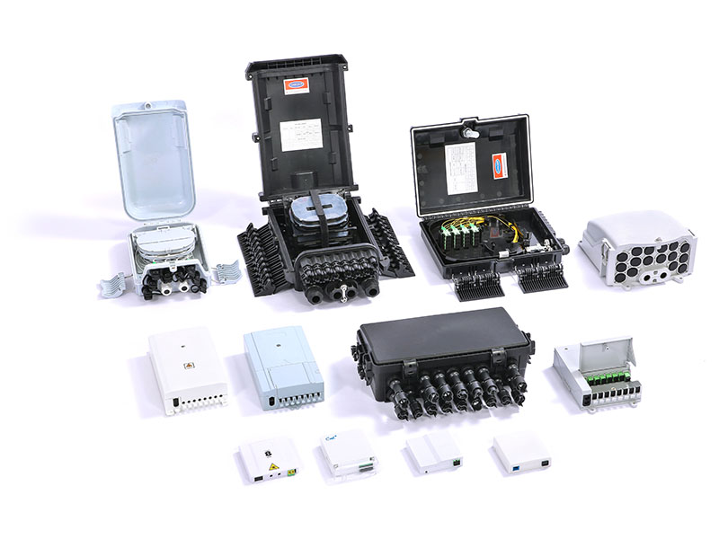
DOWELL is China's famous plc splitter manufacturer and optical splitter manufacturers. If you have any needs, please contact us!